
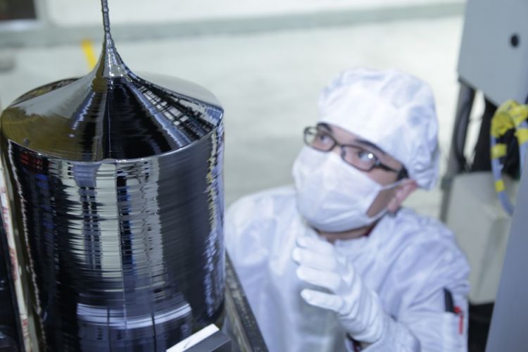
Updated: A total of seven China-based PV manufacturers have officially started efforts to establish a new ‘M10’ (182mm x 182mm p-type monocrystalline) large-area wafer size standard to reduce manufacturing costs throughout the entire solar industry supply chain as the number of large-area wafer sizes have emerged in the last few years.
Signatories to the proposed M10 wafer standard size and manufacturing specifications to China’s standards body includes leading ‘Solar Module Super League’ (SMSL) member JinkoSolar and others, including the likes of JA Solar, LONGi Group and Canadian Solar. Other PV manufacturing signatories include Jiangsu Runyang Yueda Photovoltaic Technology Co, Jiangsu Zhongyu Photovoltaic Technology and Lu’an Solar Technology Co.
The joint initiative has come at a time when the once standard M1 wafer size (156.75mm x 156.75mm) is being phased out by major wafer producers in China with large-area wafers such as that adopted by a large number of companies, initially driven by the likes of JinkoSolar to adopt the 158.75mm x 158.75mm wafer size as it suited existing cell manufacturing equipment and wafer handling limitations.
However, leading mono-wafer producer, LONGi Green Energy Technology and major merchant solar cell producers Aiko Solar and Tongwei Group started offering 161.75mm x 161.75mm. Large-area wafers of 166mm x 166mm followed shortly after.
Rivals split over large-area wafers
Then in late 2019, competitor Tianjin Zhonghuan Semiconductor (TZS) officially launched the largest wafer sizes to date in sizes of 205mm x 205mm and 210mm x 210mm, dubbed M12. They are produced from 300mm diameter mono ingots, used in the semiconductor industry.
At the time SMSL member Risen Energy had already announced 500Wp modules featuring M12 wafers and soon after TZS unveiled the M12 wafers, SMSL member, Trina Solar also announced it would be launching PV modules using that size.
At SNEC 2019, Trina Solar and many other PV manufacturers had settled on the 158.75mm wafer size due to manufacturing line compatibility and module dimensions and weight (glass/glass) versions to operate with minimal issues with the latest mounting system and single-axis tracker designs.
However, Trina Solar has recently announced the global launch of ‘TrinaPro Mega,’ the latest version of its PV utility-scale complete turnkey product solution featuring modules with power output exceeding 500W, notably its ‘Vertex’ ultra-high-power module, which launched earlier in 2020.
TrinaPro Mega’s single-axis tracker system has been specifically designed for a new era of larger and higher output modules for downstream PV power plant projects.
But it is currently unclear which large-area wafer size SMSL member GCL-SI will adopt, although sister company GCL-Poly has been closely tied to TZS on large-area mono wafer manufacturing.
Not surprisingly, the team in the M10 standardization effort have highlighted that without a new common standard there would also be an inevitable increase in manufacturing costs for auxiliary materials such as glass, whilst also making downstream selection and installation processes far more complicated.
In last weeks PV Tech’s TechTalk Series webinar with JA Solar, highlighted at length the various wafer sizes on the market and what these sizes meant to PV power plant projects as well as launch their DEEPBLUE 3.0 modules, which will use the newly formed M10 (182mm x 182mm) large-area wafers.
In a ‘soft’ launch of LONGi Solar’s HI MO5 module in late May 2020, the SMSL touted 180mm plus wafers as part of achieving 540Wp performance.
The issue then is when will M10 wafers be used in high-performance modules?
JA Solar said that it expected to begin production of its DEEPBLUE 3.0 modules in the third quarter of 2020 with an anticipated production capacity of 14GW. The company has made a number of capacity expansion announcements since the beginning of 2020, including plans to expand its monocrystalline silicon ingot capacity by 10,000MT at its subsidiary in Xingtai Economic Development Zone, Hebei province, China.
In many respects, M10 wafers used in PV modules are expected to start ramping to volume production in the fourth quarter if 2020 and become widely available in the first-half of 2021.